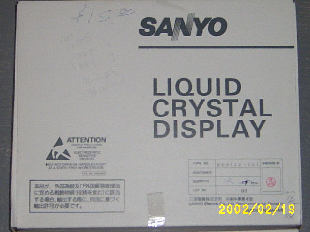
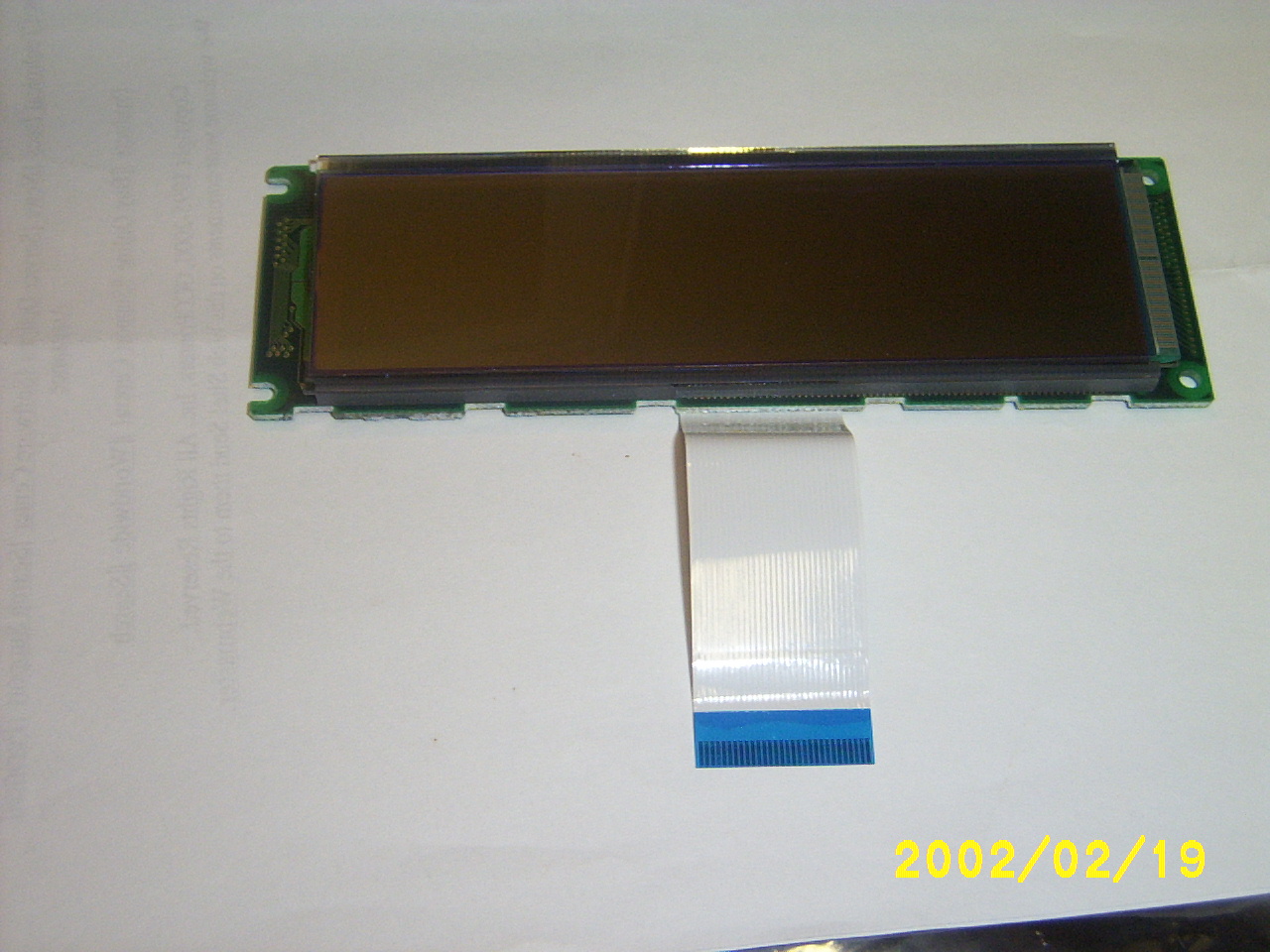
Here is a short description of the DG071Z lcd display I fell over.
I'm working on a better page but since that will take awhile (as in maybe never) I decided
to just scribble down my notes (before I loose them) here for a start.
Most
of the info is based on my tests with a multimeter. If a pin goes from
U1-1 to U2-2 it can also go to U3-3 since I didn't check every
possibility everywhere.
What I found out so far;
If you have more info, corrections, questions etc., send an email to; <peters AT techwiz.ca>
The documentation I have is:
Toshiba T6963C Technical description
Toshiba T6963C Application Notes
Comments to the Toshiba doc
Sample program in C (for another LCD display)
Lcd driver LC7940ND/LC7941ND
Lcd driver LC7942ND
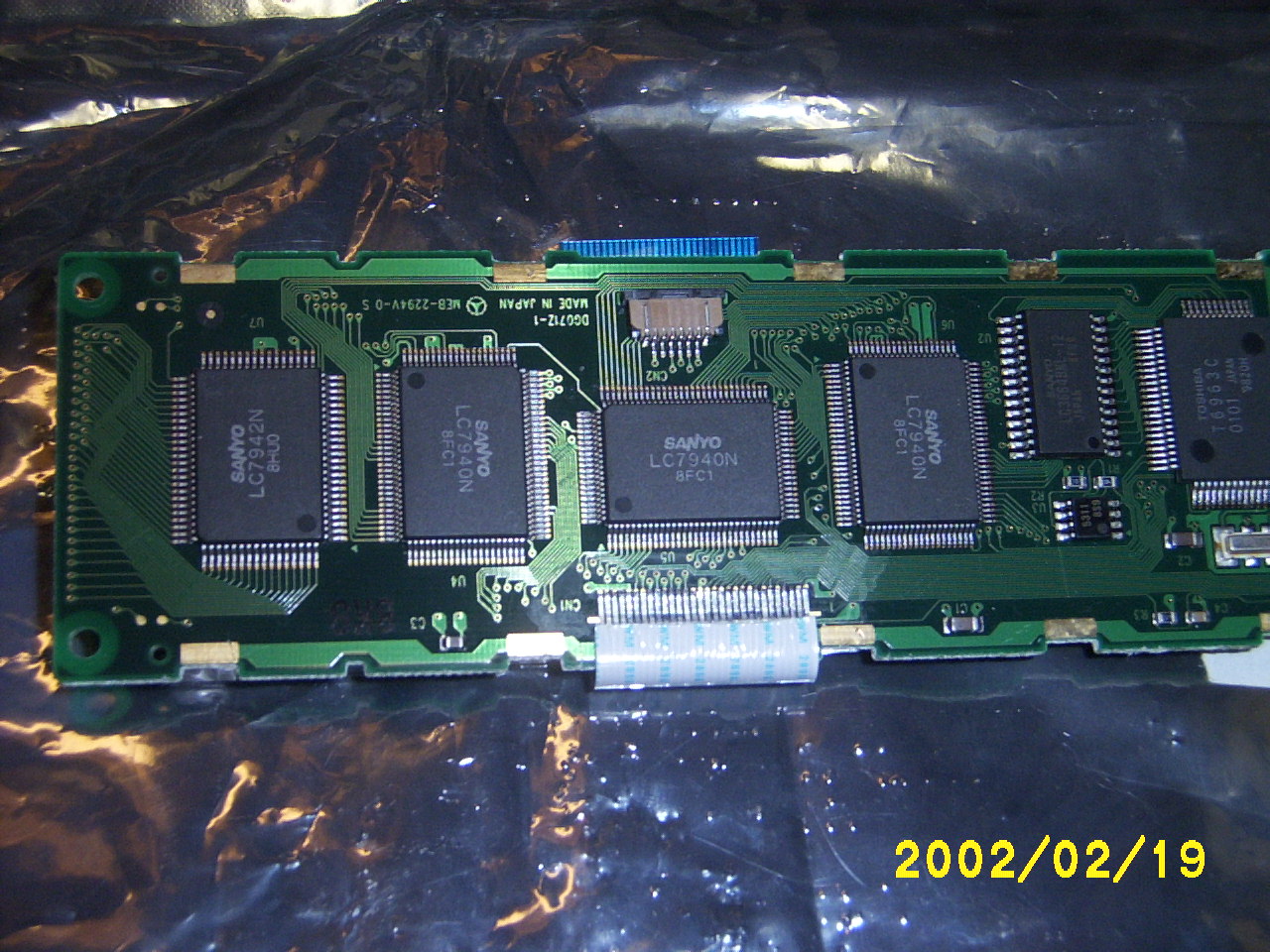
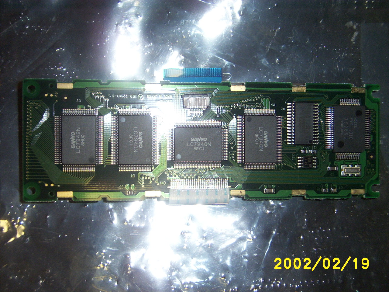
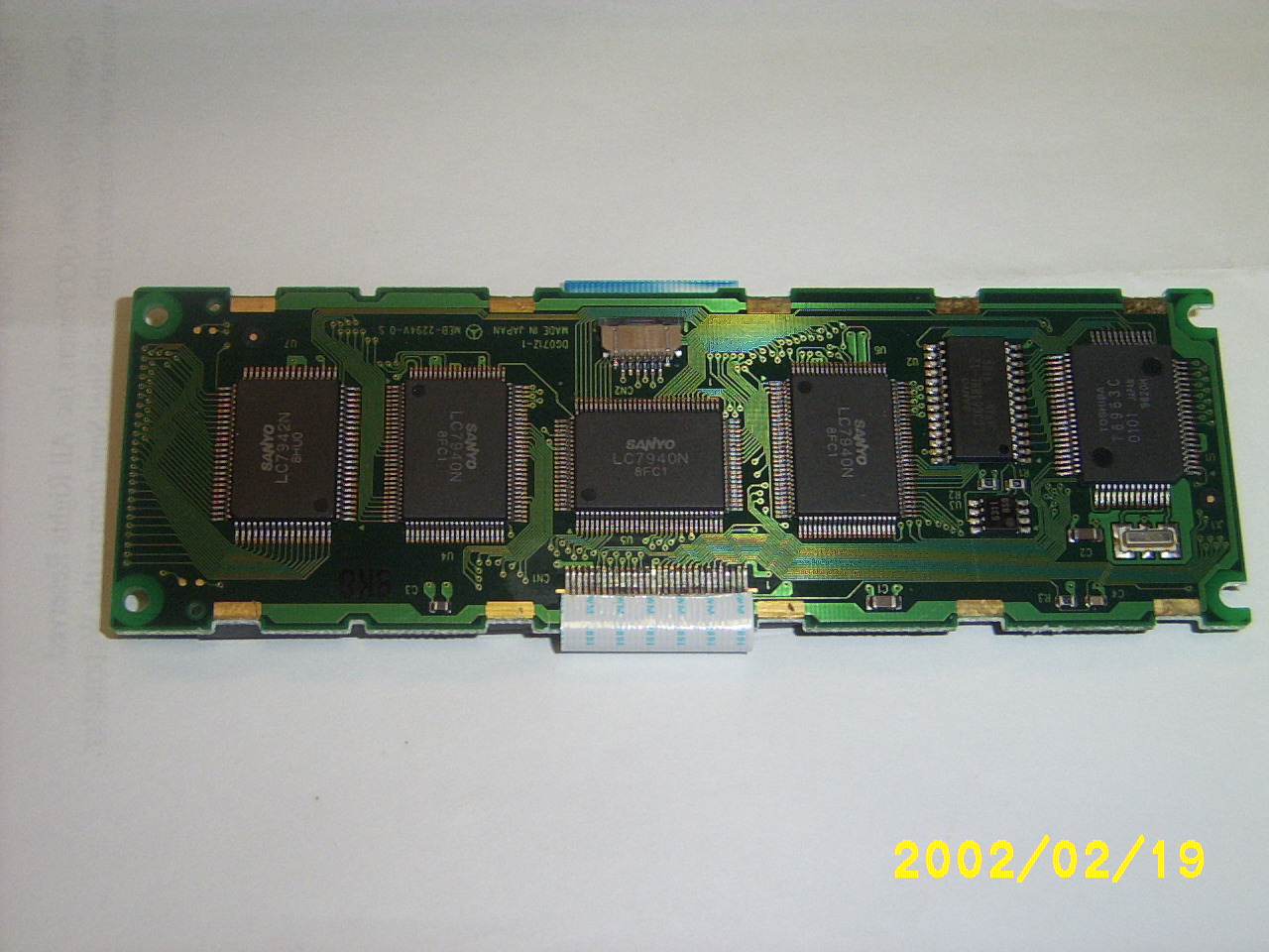
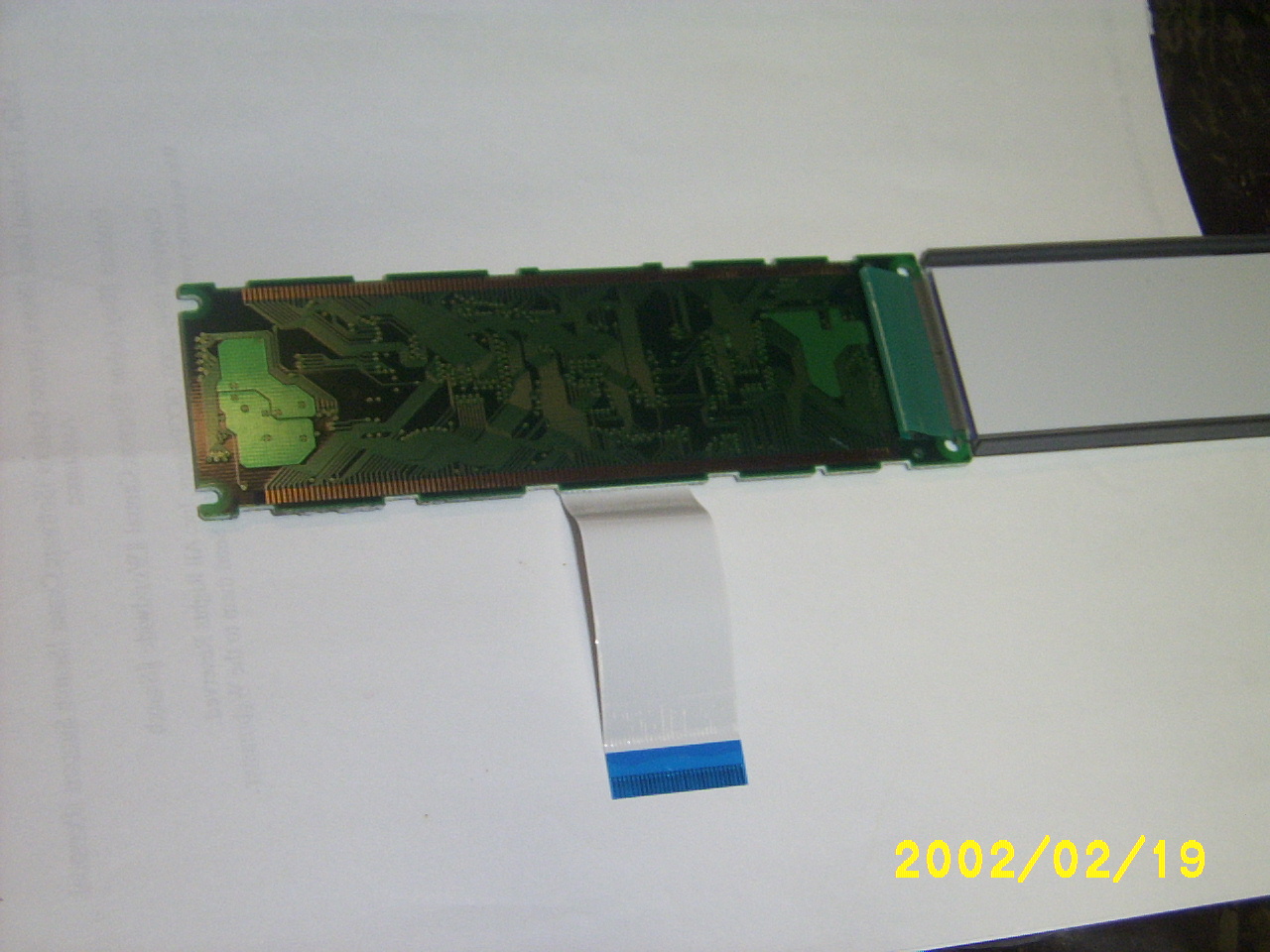
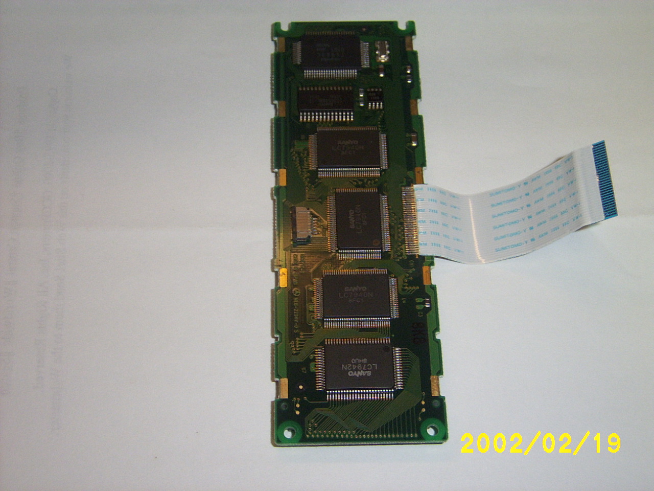
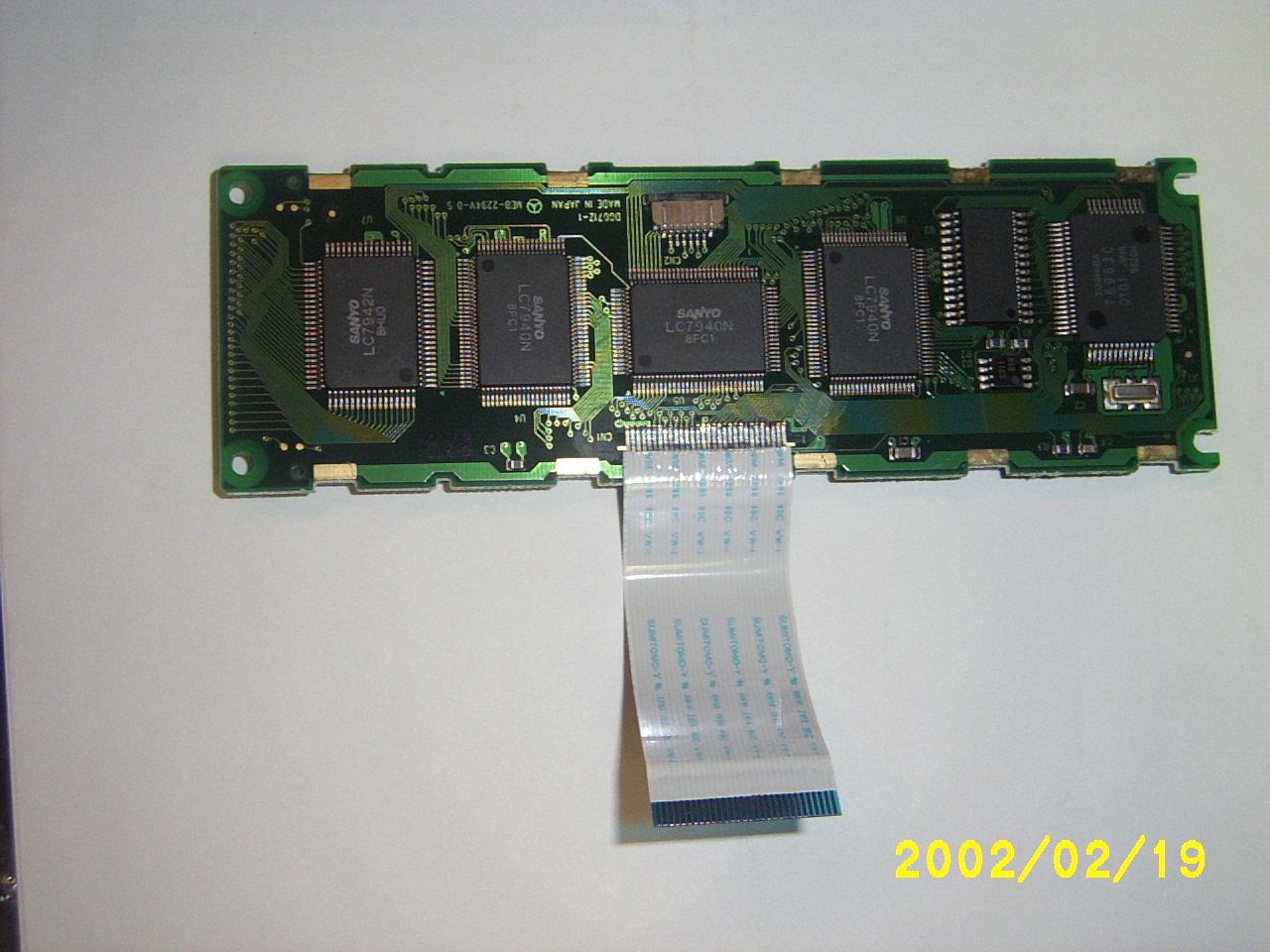
The unit has a few components.
| CN1 | Flat Cable | Main connection |
| CN2 | Small Connector | |
| U1 | T6963C | LCD Controller |
| U2 | LC3664BML-12 | 8Kx8 Ram |
| U3 | 8S9 | LCD Power module (?) |
| U4 | LC7940 | LCD Driver X |
| U5 | LC7940 | LCD Driver X |
| U6 | LC7940 | LCD Driver X |
| U7 | LC7942 | LCD Driver Y |
| X1 | 400??? | Can't read what's stamped on it |
All values are measured on the board so they are only guidelines.
| C1 | 205nF |
| C2 | 95nF |
| C3 | 268nF |
| C4 | 230nF |
| R1 | 97ohm |
| R2 | 99ohm |
| R3 | 4K46ohm |
Here comes some schematics extracts
CN1 is the flat cable
CN2 is the small one on top
CN1-1 = Connectior 1, pin 1
Vdd
|
R3
U1 Reset ----+-----CN1-3
C4
|
Vss
Vdd Vdd
|
|
C1
C3
|
|
Vss
Vss
| CN1-1 | Vdd | ||
| CN1-2 | Vss | ||
| CN1-3 | U1-2 | Reset | |
| CN1-4 | U1-10 | D0 | |
| CN1-5 | U1-11 | D1 | |
| CN1-6 | U1-12 | D2 | |
| CN1-7 | U1-13 | D3 | |
| CN1-8 | U1-14 | D4 | |
| CN1-9 | U1-15 | D5 | |
| CN1-10 | U1-16 | D6 | |
| CN1-11 | U1-17 | D7 | |
| CN1-12 | U1-18 | WR | |
| CN1-13 | U1-19 | RD | |
| CN1-14 | U1-20 | CE | |
| CN1-15 | U1-21 | C/D | |
| CN1-16 | |||
| CN1-17 | Frame ground | ||
| CN1-18 | CN2-1 | ||
| CN1-19 | CN2-2 | ||
| CN1-20 | CN2-6 | ||
| CN1-21 | CN2-3 | ||
| CN1-22 | CN2-4 | ||
| CN1-23 | CN2-5 | ||
| CN1-24 | U7-31 | Disp Off | |
| CN1-25 | U1-9 | FS1 | Select 6x8 or 8x8 font |
| CN1-26 | Vss | ||
| CN1-27 | Vss | ||
| CN1-28 | Vss | ||
| CN1-29 | Vss | ||
| CN1-30 | Vss |
| mds | Vss | |
| md0 | Vss | |
| md1 | Vss | |
| md2 | Vss | |
| md3 | Vdd | |
| fs0 | Vss | |
| fs1 | CN1-25 | |
| D0-D7 | CN1-4 to 11 | |
| WR | CN1-12 | |
| RD | CN1-13 | |
| CE | CN1-14 | |
| C/D | CN1-15 | |
| d0-d7 | U2-11 to 19 | |
| Vdd | VN1-1 | |
| r/w | U2-27 | |
| ec | u2-21 | |
| ad0-7 | u2-10 to 3 | |
| ad8-11 | n/c? | |
| ad12 | U2-2 | |
| ad13-15 | n/c? | |
| HOD | ? | |
| ED | U4-97 | SDI |
| HSCP | U4/5/6-100 | CP |
| DUAL | Vss | |
| LP | U4/5/6-98 | LOAD |
| CDATA | U7-25 | DIO64 |
| FR | U4/5/6-93 & U7-36 | M |
| CH1 | ? | |
| CH2 | ? | |
| DSOPN | ? | |
| Vdd | Vdd | |
| SDSEL | Vss | |
| Vss | Vss | |
| T2 | ? | |
| T1 | ? | |
| X1 | X1 | |
| X0 | X1 |
| 1 | Vdd | V1 |
| 2 | U7-29 | V2 |
| 3 | U4/5/6-89 | V3 |
| 4 | <R1>-U3-5 | |
| 5 | <R1>-U3-4 | |
| 6 | U4/5/6-88 | V4 |
| 7 | U7-28 | V5 |
| 8 | -<R2>-U7-27 | Vee |
| 8 | -<C2>-Vss |
U4-CDI Vss
U4-CDO -> U5 CDI
U5-CDO -> U6 CDI